Silicon wafers account for roughly 40% of semiconductor manufacturing costs, but a breakthrough in crystal growth technology could slash those expenses dramatically. Researchers at multiple universities have developed methods to grow ultra-pure silicon crystals in laboratory settings at a fraction of traditional costs, potentially revolutionizing chip production worldwide.
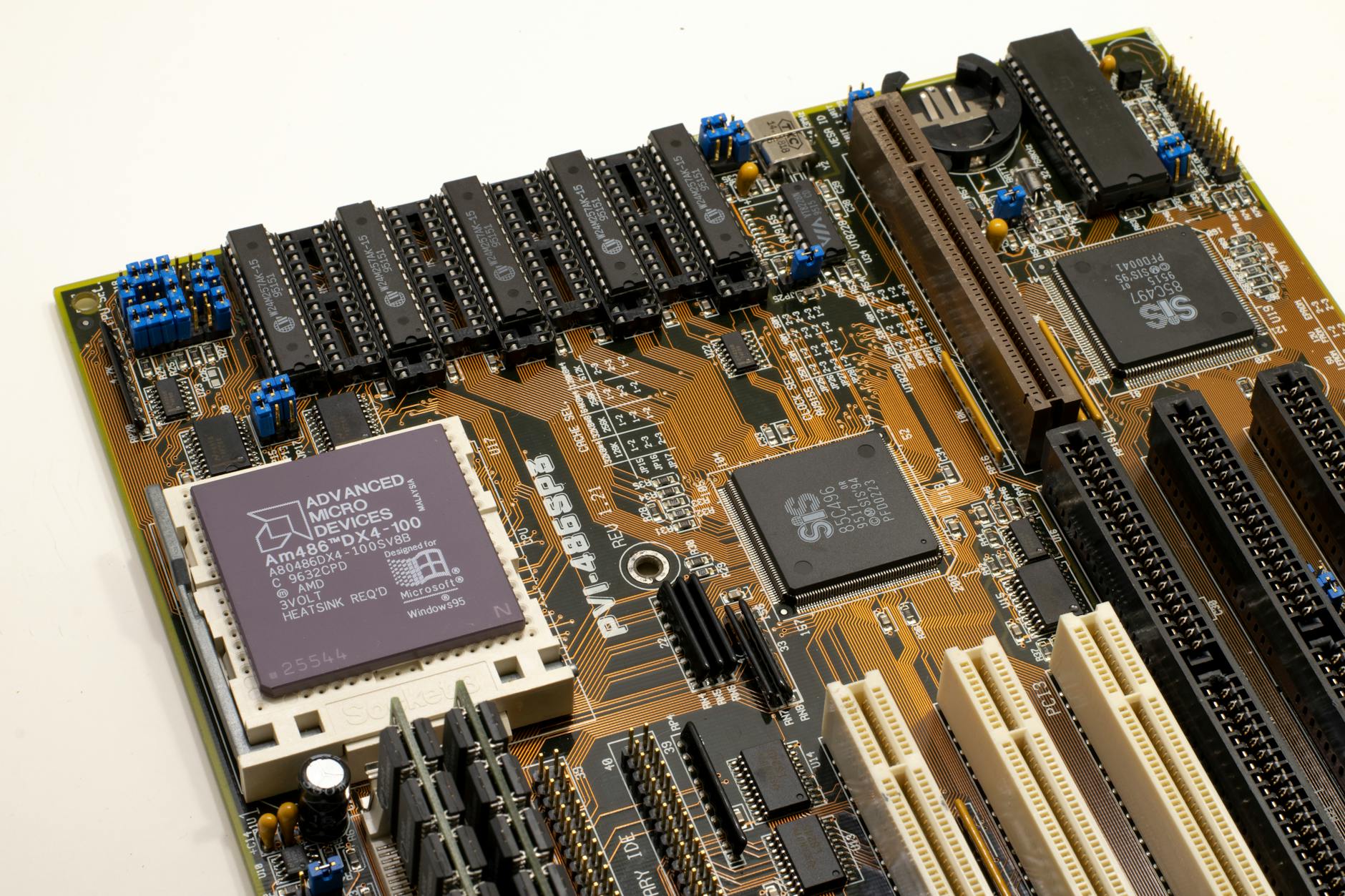
The semiconductor industry has relied on the Czochralski process for decades, pulling single crystals from molten silicon to create the wafers that form the foundation of every computer chip. This energy-intensive method requires temperatures exceeding 1400 degrees Celsius and specialized equipment that costs millions of dollars to operate.

New Crystal Growth Methods Show Promise
Teams at MIT, Stanford, and several international institutions have been experimenting with alternative approaches to silicon crystal formation. Their techniques involve growing crystals at lower temperatures using seed layers and controlled chemical vapor deposition processes.
The most promising method involves creating silicon crystals on specially prepared substrates at temperatures around 600 degrees Celsius. This represents a significant reduction in energy requirements compared to traditional methods. The process uses precise control of silicon-containing gases to build up crystal structures layer by layer, similar to how 3D printing creates objects.
Initial results suggest these lab-grown crystals can achieve purity levels comparable to conventionally produced silicon wafers. The key breakthrough lies in the controlled environment that eliminates many of the impurities that typically contaminate silicon during high-temperature processing.
Several companies are now investing in pilot programs to scale up these laboratory techniques. Intel, TSMC, and Samsung have all reportedly allocated research funds to explore alternative silicon production methods as chip demand continues to surge globally.
Cost Reduction Potential Attracts Industry Attention
The financial implications of cheaper silicon production extend far beyond semiconductor manufacturers. Lower wafer costs could reduce prices for everything from smartphones to automotive chips, potentially making advanced computing more accessible worldwide.
Current silicon wafer prices fluctuate based on supply and demand, but typically range from hundreds to thousands of dollars per wafer depending on size and quality specifications. The new crystal growth methods could potentially cut these costs by 30 to 50 percent once scaled to industrial production levels.
Energy costs represent another significant factor driving interest in these alternatives. Traditional silicon crystal growing consumes enormous amounts of electricity to maintain the extreme temperatures required for the Czochralski process. Lower-temperature alternatives could reduce the carbon footprint of semiconductor manufacturing substantially.
The timing proves crucial as global chip demand continues expanding. Electric vehicles, artificial intelligence systems, and Internet of Things devices all require massive quantities of semiconductors. Any technology that can increase production capacity while reducing costs addresses two critical industry challenges simultaneously.
Similar innovations in materials science are emerging across multiple sectors. Lab-grown wood alternatives could replace plastic in electronics manufacturing, demonstrating how synthetic materials are transforming traditional industries.
Technical Challenges Remain
Despite promising initial results, scaling laboratory crystal growth to industrial production presents significant hurdles. The controlled environments required for consistent crystal quality are difficult to maintain in large-scale manufacturing facilities.
Uniformity across large wafer surfaces remains problematic with current techniques. Traditional Czochralski-grown crystals benefit from decades of process refinement, achieving extremely consistent properties across entire wafer surfaces. New methods must match this reliability before commercial adoption becomes viable.
Quality control systems need development to ensure lab-grown crystals meet the exacting standards required for advanced semiconductor devices. Modern processors require silicon purity levels exceeding 99.9999%, with crystal defects measured in parts per billion.
Equipment manufacturers are working to adapt existing production lines to accommodate new crystal growth processes. This transition requires substantial capital investment and extensive testing to validate that new methods produce chips with identical performance characteristics.
Market Implications and Timeline
Industry analysts predict commercial implementation of alternative silicon crystal growth could begin within the next five years, assuming current research trends continue. However, widespread adoption will likely take longer as manufacturers validate new processes and retool production facilities.
The geopolitical implications could prove significant as well. Countries seeking to establish domestic semiconductor manufacturing capabilities might find lower-cost production methods more attractive than traditional approaches requiring massive initial investments.
Several startups have emerged focusing specifically on alternative silicon production methods, attracting venture capital funding and partnerships with established chip manufacturers. These companies aim to commercialize laboratory techniques and bridge the gap between academic research and industrial application.
Competition between traditional and alternative production methods could drive further innovation across the entire semiconductor supply chain. Established silicon producers are responding by investing in their own research programs to improve existing processes and reduce costs through other means.
The success of lab-grown silicon crystals could accelerate broader trends toward synthetic materials in technology manufacturing. As industries seek more sustainable and cost-effective production methods, laboratory-grown alternatives may become increasingly common across multiple sectors.
Silicon crystal growth represents just one area where advanced materials science is reshaping manufacturing possibilities. The combination of lower costs, reduced environmental impact, and potentially higher quality could make lab-grown silicon crystals a transformative technology for the global electronics industry.
Frequently Asked Questions
How much could lab-grown silicon reduce chip manufacturing costs?
Research suggests lab-grown silicon crystals could reduce wafer costs by 30-50% compared to traditional methods.
When will lab-grown silicon be commercially available?
Industry analysts predict commercial implementation could begin within five years, with widespread adoption taking longer.